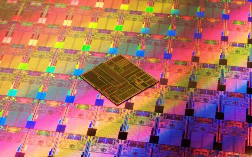
TSMC, the foundry that produces the SoC A10 Fusion, A11 Bionic, and A12 Bionic of the last generation of iPhone was already one of the first with HiSilicon to offer chips engraved in 7nm. The smelter is also well positioned to be a precursor to the 5nm etching process. In a statement TSMC announces the delivery of the first "infrastructure for technology [engraving] 5nm process". For the time being, this means that the firm has completed the Design Rule Manual, models, industrial design kits, silicon processing processes and connection interfaces, as well as "a full range of tools EDA and design processes ".
TSMC Announces Ready for 5nm SoCs
The first SoC engraved in 5nm would thus be available by 2020: "compared to the TSMC 7nm process, its innovative scale features deliver a 1.8x higher logical density and a 15% speed gain on an ARM core. Cortex-A72, "says TSMC. The manufacturer of the Apple Axx chips will also pass this year to the 7nm + process - an improved 7nm process with EUV technology that already allows a significant increase in density, of the order of 20% and a reduction in energy consumption up to 'at 12%. Production should begin at the beginning of the year, we can hope to find this process 7nm + manufacturing in Apple A13 chips within a few months.
The success or failure of TSMC in these new manufacturing processes should have implications in the industry. A rather tight order of founders maintains control over the industry. TSMC's client is Apple, but also Nvidia and AMD. It remains to be seen whether the smelter will be able to push the limits of silicon beyond 5nm. What already represents an extreme level of detail, with components that can make only 1nm is barely 5 silicon atoms wide. After the engraving 5nm comes the engraving in 3nm, and beyond. A finesse that will probably involve, then, to find an alternative to silicon.

